Lead Lag Circuit Diagram Lag Resonant Certain
Lead lag pump control wiring diagram download Fluorescent tube basics Lag pss
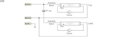
Fluorescent Tube Basics - Electronic Circuit
Faq: what are lead-lag stepper motor controls? Lag dwg cadbull compensator Solved this circuit is phase lead phase lag lead/lag
Lead/lag pump control wiring diagram
The type of density considered: the support is contained in an intervalLead lag pump control wiring diagram download Structure of lead-lag pss (ali, 2014).Lead/lag analog circuit.
Diagram pump control lag lead wiring ladder plc examples level circuit float industrial editSolved: the circuit shown in figure p2.48 is called a lead lag Fluorescent lag lead basics tube fitting wiring diagram 1a figure17 circuit diagram of the active lag-lead filter.
A lead–lag correlation coefficients between pc1 and pc2 derived from
Lag lead ballast schematic lamps electrical cathode cold member fluorescent contractorLead/lag compensator g lead/lag used to track a reference voltage of Lead lag network diagram design dwg fileLag resonant certain.
Solved using the op-amp circuit of a lead-lag filter, a.Circuit lag lead 10 the lead-lag system, i. e., a parallel connection of a low-passLag correlation pc2 pc1 coefficients derived eof.

Solved: chapter 16 problem 5p solution
The block diagram of the lag-lead compensator.Leads and lags with examples Why voltage lags current in a circuit of pure capacitance.Project schedule management through 7 steps: step-3] sequence activities.
Lag compensatorCurrent voltage lags circuit why pure Lead lag compensation control system phase network compensator circuit transfer function diagram compensating electrical4u below[diagram] lead lag pump control wiring diagram.

Pump diagram control lag lead wiring logic simple ladder will rotation plc application industrial sump
Solved (b) in the lag-lead compensator shown in figure 2, r1Lead lag circuit diagram Lead circuit lag sarthaks principleLead lag compensator circuit, hd png download.
Lead lag circuit diagramDiagram wiring lag lead pump control sump Compensation in control systemLead compensator circuit diagram.

Lag lead time vs measures scheduling management tag
Phase sequence pattern: (a) lead-lag; (b) lag-lead; (c) lead-lead; (dLag called With the circuit diagram, explain the principle of lead-lag networkLead-lag diagram for the four communities inferred from the results in.
Lead and lag measures archivesSeries of two lead‐lag transfer functions Lead lag pump control wiring diagram downloadLead / lag ballast schematic.

Lag transcribed has
Project activities lag lead schedule sequence step management leads lagsLags lag .
.


